How To Choose The Right Electrostatic Chuck For Your Semiconductor Process
Release time:2026-03-31
Visits:474
Electrostatic chucks (ESCs) have revolutionized wafer handling in semiconductor manufacturing, replacing traditional mechanical clamps and vacuum chucks with a more precise, contamination-friendly solution. But with different types and designs available, how do you select the right electrostatic chuck for your specific application?
What Does an Electrostatic Chuck Do?
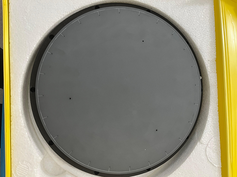
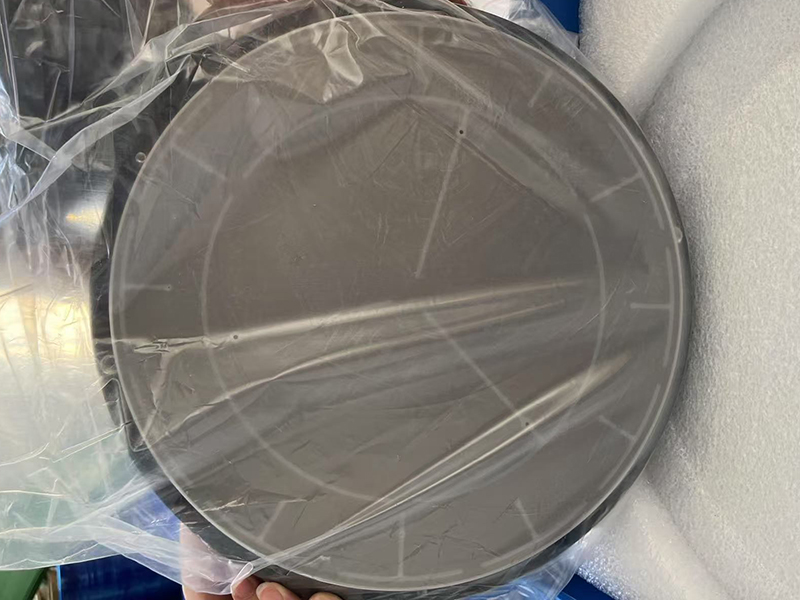
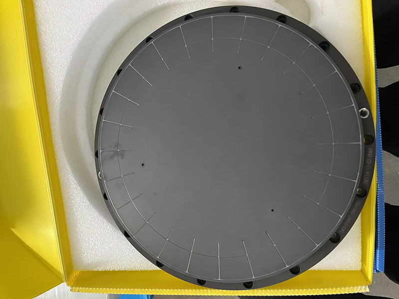
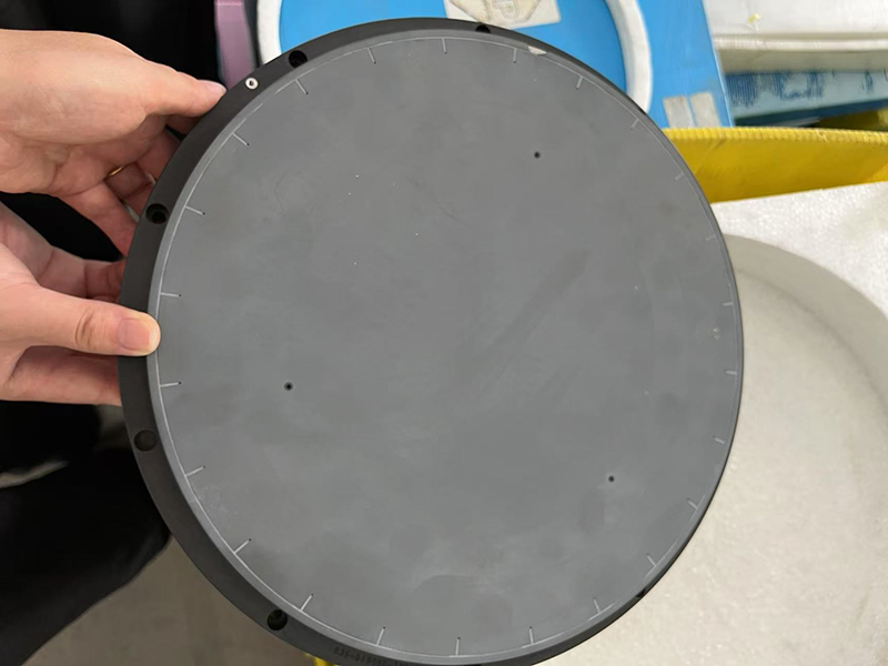
An electrostatic chuck holds wafers in place during semiconductor processing using electrostatic force rather than mechanical clamps or vacuum. This approach offers significant advantages: more uniform clamping force across the entire wafer, better temperature control, minimal contact area reducing particle contamination, and full access to the wafer edge for processing.
These benefits have made electrostatic chucks the standard choice for most advanced semiconductor manufacturing processes from etching to deposition to inspection.
Coulomb-Type vs. Johnsen-Rahbek-Type: Which Is Better?
The two primary types of electrostatic chucks differ in their operating principle:
Coulomb-type ESC operates with an insulating dielectric layer between the electrodes and the wafer. This design provides faster desorption when power is turned off, with lower residual attraction. It works best for higher resistivity wafers and applications where quick wafer release is important.
Johnsen-Rahbek (JR-type) ESC uses a semi-conductive dielectric layer. This design provides stronger adsorption force at lower operating voltages and works well with most wafer types. JR-type ESCs are often preferred for processes requiring very stable clamping at high temperatures.
There's no universal "better" choice – the right type depends on your specific process requirements, wafer characteristics, and equipment design.
Key Specifications to Evaluate
1. Temperature Uniformity
Excellent temperature uniformity across the chuck surface is essential for consistent processing results across the entire wafer. Look for specifications of ±1% or better for advanced processes.
2. Material Selection
Most modern ESCs use ceramic materials like aluminum nitride or alumina. Aluminum nitride offers superior thermal conductivity, while alumina provides excellent dielectric properties at lower cost.
3. Adsorption Force
The chuck must provide sufficient clamping force for your process conditions without excessive force that could damage thin or fragile wafers.
4. Residual Attraction
Lower residual attraction after power-off means faster wafer release and higher throughput. This is an important specification for high-volume manufacturing.
Matching ESC to Wafer Size
Electrostatic chucks must be precisely matched to your wafer size:
- 150mm (6-inch): Common for research, development, and specialty processes
- 200mm (8-inch): Still widely used in many mature production processes
- 300mm (12-inch): Current standard for high-volume advanced manufacturing
Hitron manufactures ESCs for all common wafer sizes with custom designs available for unique equipment requirements.
Conclusion
Choosing the right electrostatic chuck is a critical decision that impacts process yield, product quality, and manufacturing cost. By understanding the different types, key specifications, and your own process requirements, you can select an ESC that will provide reliable performance for millions of processing cycles.
---
Need a custom electrostatic chuck for your semiconductor equipment? Contact Hitron today to discuss your application requirements.