Analysis Of Technical Advantages And Industrial Applications Of ESC Electrostatic Chucks
Release time:2026-01-23
Visits:198
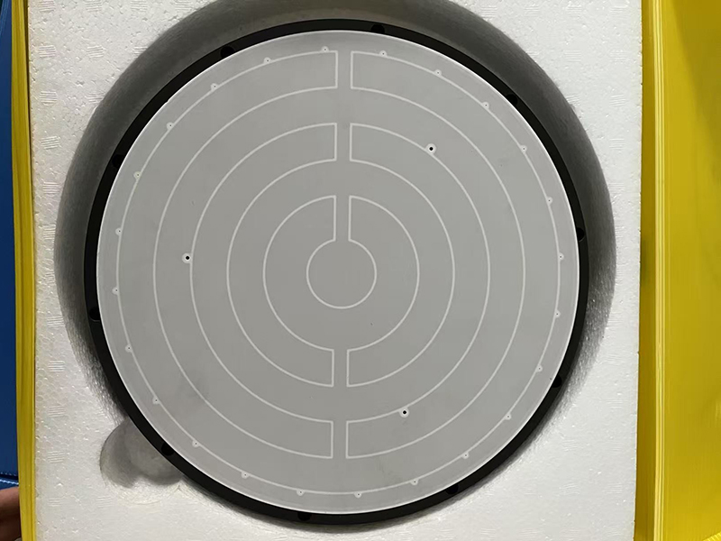
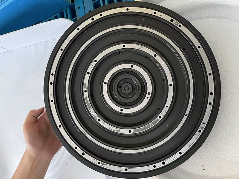
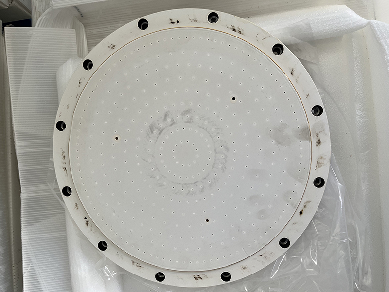
As a new type of precision clamping technology replacing traditional mechanical clamping and vacuum adsorption, ESC Electrostatic Chucks have been applied on a large scale in various high-end manufacturing fields such as semiconductors, panel displays, solar photovoltaics and precision optics by virtue of their unique technical advantages, and have become the core carrier for modern ultra-clean thin sheet processing.
Compared with traditional clamping methods, the core technical advantages of ESC Electrostatic Chucks are reflected in four major aspects.
First, non-contact and stress-free clamping: Fixation is achieved by electrostatic force without physical contact, which completely avoids wafer damage and edge exclusion effect caused by mechanical fixtures, and is suitable for the processing of ultra-thin wafers with a thickness of less than 50μm and brittle semiconductor materials such as GaN and SiC.
Second, full environmental adaptability: It can work stably under various working conditions such as atmospheric pressure, ultra-high vacuum and plasma, and can adsorb conductors, semiconductors, insulators and porous materials, with an extremely wide scope of application.
Third, low consumption and high cleanliness: The energy consumption of electrostatic adsorption is much lower than that of vacuum adsorption equipment. In addition, no electric potential is generated on the back of the workpiece during the adsorption process, so it will not adsorb surrounding dust and particles, meeting the ultra-clean requirements of semiconductor processes.
Fourth, controllable and easy operation: It can realize rapid adsorption and release with stable and precisely adjustable clamping force. Cooperating with a customized controller, it can minimize the unclamping time and improve the overall process operation efficiency.
In industrial applications, ESC Electrostatic Chucks are core components in front-end semiconductor manufacturing. In processes such as etching, ion implantation and CVD/PVD thin film deposition, they ensure the positional fixation and temperature uniformity of wafers in extreme environments, which directly affect the precision and yield of chip manufacturing. In the panel industry, they are used for the flat clamping of glass substrates in vacuum lamination processes to avoid wrinkles and air bubbles during lamination. In the fields of solar photovoltaics and precision optics, they can realize the soft support and high-precision processing of thin workpieces such as silicon wafers and optical lenses.
Meanwhile, ESC Electrostatic Chucks can work in coordination with equipment such as vacuum hot presses. In emerging processes such as advanced semiconductor packaging and Chiplet integration, through the synergy of multi-physical fields including non-contact fixation, vacuum, precise temperature control and uniform pressure, they solve the bottleneck problems of traditional processes such as oxidation, air bubbles and stress damage. With the development of semiconductor processes towards greater miniaturization and integration, ESC Electrostatic Chucks are being upgraded in the direction of high precision, high thermal conductivity and modular customization.