Core Product Introduction Of ESC Electrostatic Chuck
Release time:2026-01-23
Visits:267
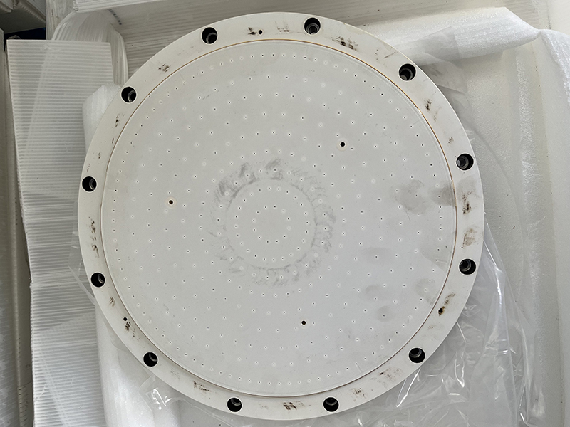
The ESC Electrostatic Chuck is a core wafer clamping device in the field of semiconductor manufacturing, with electrostatic adsorption as its fundamental principle. It forms an electrostatic field by applying a high voltage and achieves non-contact fixation of wafers through Coulomb force or Johnson-Rahbek force, serving as an indispensable key component in vacuum processes such as plasma etching, ion implantation and thin film deposition.
This product is adapted to harsh process environments including non-magnetic conditions and ultra-high vacuum of 10⁻⁵ Pa and below, and can stably adsorb various dielectric materials such as wafers, sapphire and glass. It supports customized designs of bipolar, multipolar and interdigitated electrodes, with the global flatness accuracy of the adsorption surface reaching within 1μm and parallelism better than 5μm. The adsorption force is ≥10N under the standard adsorption voltage, and the residual adsorption force remains above 60% for 24 hours, enabling the maintenance of a stable clamping effect for an extended period.
In terms of structure and performance, the ESC Electrostatic Chuck is coated with high thermal conductivity ceramic films such as aluminum nitride and silicon nitride, which combines excellent plasma corrosion resistance and mechanical strength. Some high-end products integrate multi-zone temperature control electrodes and a backside helium cooling system to achieve precise and uniform regulation of wafer temperature, avoiding wafer warpage or uneven thin film deposition caused by thermal stress. Meanwhile, its adsorption force is evenly distributed without local stress points, which can effectively protect the surface integrity of fragile materials such as ultra-thin wafers and precision optical components, and eliminate scratches and deformation issues caused by mechanical clamping.
At present, the ESC Electrostatic Chuck has become a core component of ultra-large-scale integrated circuit manufacturing equipment, and is widely applied in processes such as wafer metrology, electron beam lithography and semiconductor chip packaging. Moreover, parameters including the number of electrodes, flatness specifications and overall dimensions can be custom-designed according to process requirements, adapting to processing scenarios of wafers with different specifications such as 8-inch and 12-inch.