What Is an Electrostatic Chuck (ESC)?
An
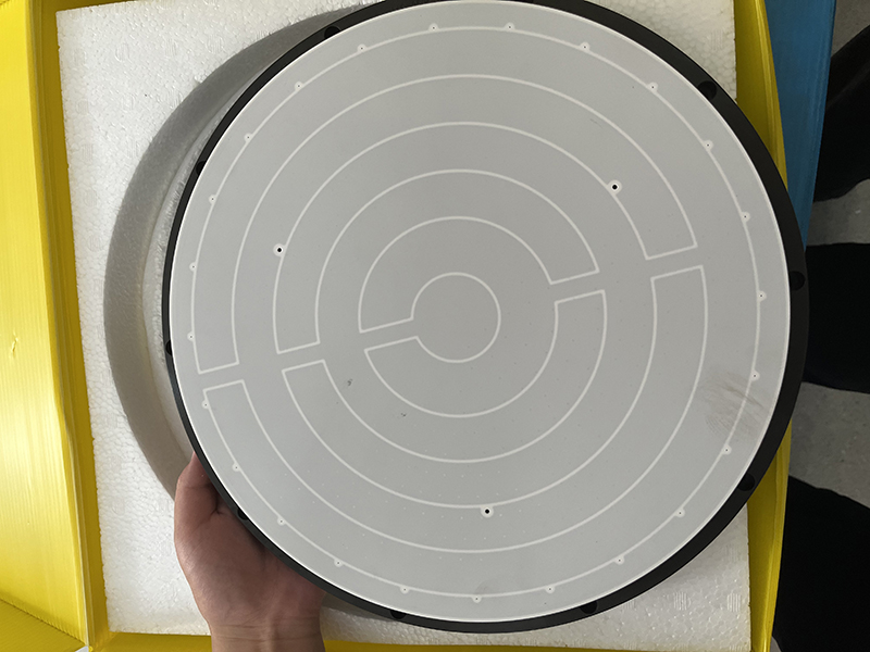
electrostatic chuck (ESC) is a ceramic or metal-based wafer-holding substrate used inside plasma process chambers that uses an electrostatic field to clamp a silicon (or other) wafer against a thermally-controlled pedestal, replacing mechanical clamping for sub-micron overlay accuracy and backside gas cooling. ESCs were introduced in the 1980s and have become universal in 200 mm and 300 mm etch, CVD, PVD, and ion-implant tools.
Typical ESC applications:
Plasma etch (dielectric and metal etch).
Plasma-enhanced CVD (PECVD) and high-density plasma CVD (HDPCVD).
Physical vapor deposition (PVD / sputtering).
Ion implantation (high-current and medium-current).
Atomic layer deposition (ALD).
Plasma doping (PLAD).
The combination of high clamping force (> 50 g/cm² typ.), uniform thermal contact, no mechanical edge ring, and compatibility with vacuum and plasma environments makes ESC the standard wafer-holding technology for advanced-node semiconductor manufacturing.
How Does an ESC Work?
An ESC uses a thin dielectric layer (ceramic or polymer) with one or two embedded electrodes to which a high DC voltage (typ. ±600 to ±1500 V) is applied, creating an electrostatic attraction that clamps the wafer against the chuck surface. The clamping force depends on voltage, dielectric thickness, and chuck / wafer interface.
Two main ESC mechanisms:
Coulombic ESC. Thick dielectric layer (typ. > 100 μm), low leakage, slow clamp / release (typ. seconds).
Johnsen-Rahbek (J-R) ESC. Thin dielectric or slightly conductive ceramic (typ. 10–50 μm leakage path), fast clamp / release (< 100 ms), higher leakage current.
|
Mechanism |
Dielectric |
Clamp speed |
Leakage |
Application |
|
Coulombic |
Al₂O₃, AlN, ceramic |
Slow (typ. 1–5 s) |
Very low |
High-temperature, ion implant |
|
Johnsen-Rahbek |
Doped ceramic, slightly conductive |
Fast (< 100 ms) |
Moderate |
Etch, CVD (fast throughput)
|
For high-throughput etch and CVD, Johnsen-Rahbek ESCs are preferred because of the fast clamp / release cycle time. For high-temperature or high-purity applications (ion implant, ALD), Coulombic ESCs are preferred.
What Are the Key ESC Specifications?
The key ESC specifications are wafer size, clamping voltage, clamping pressure, leakage current, breakdown voltage, thermal conductance, temperature range, and backside gas flow. Each specification is controlled by the chuck manufacturer to meet process requirements.
|
Specification |
Typical value (300 mm) |
Notes |
|
Wafer size |
300 mm (also 200, 150 mm) |
Determines chuck diameter |
|
Clamping voltage |
±600 to ±1500 V DC |
Depends on chuck type |
|
Clamping pressure |
30–100 g/cm² |
Higher = better thermal contact |
|
Leakage current |
< 1 mA (Coulombic), < 10 mA (J-R) |
Affects wafer damage |
|
Breakdown voltage |
> 3000 V DC |
Safety margin over operating voltage |
|
Thermal conductance |
0.1–1.0 W/cm²·K |
Heat transfer to wafer |
|
Backside gas pressure |
5–30 Torr (He) |
Heat-transfer gas |
|
Temperature range |
−50 °C to +400 °C (typ.) |
Process-dependent |
|
Temperature uniformity |
±1 °C across wafer |
Critical for etch uniformity |
|
Lifetime |
> 10,000 clamp cycles |
Replaced at end-of-life |
For advanced-node logic and memory, temperature uniformity of ±0.5 °C or better is required for high-yield etch.
What Are the Main ESC Types?
ESCs are categorized by the dielectric material, electrode configuration, and cooling method, with the most common being ceramic-alumina (Al₂O₃), aluminum-nitride (AlN), and doped ceramic, with monopolar or bipolar electrode configurations and water-cooled or chiller-cooled bases.
|
ESC type |
Dielectric |
Application |
Notes |
|
Alumina (Al₂O₃) |
Al₂O₃ ceramic |
General etch, CVD |
Standard, lower thermal conductivity |
|
Aluminum-nitride (AlN) |
AlN ceramic |
High-power etch |
High thermal conductivity |
|
Doped ceramic (J-R) |
Al₂O₃ + TiO₂ |
High-throughput etch |
Fast clamp, moderate leakage |
|
Monopolar |
Single electrode |
Simple clamp |
Requires bipolar wafer or bipolar supply |
|
Bipolar |
Two electrodes (+/−) |
Standard clamp |
More uniform force, no wafer requirement |
|
Coulombic |
Thick dielectric |
High-temperature, implant |
Slow clamp, very low leakage |
|
Johnsen-Rahbek |
Thin / doped dielectric |
High-throughput etch |
Fast clamp, moderate leakage |
For 300 mm advanced-node etch, AlN bipolar J-R ESC is the standard because it provides high thermal conductivity (170 W/m·K vs. 30 W/m·K for Al₂O₃) and fast clamp / release for high throughput.
How Is the ESC Cooled?
ESCs are cooled by backside gas (typically helium at 5–30 Torr) flowing between the wafer and the chuck surface, in combination with liquid cooling of the chuck base to a chiller set point (−50 °C to +80 °C). The backside gas conductance is the dominant thermal-transfer mechanism from the wafer to the chuck.
Thermal-transfer stack:
Wafer (front side heated by plasma).
Backside gas gap (typ. 5–30 Torr He).
Ceramic dielectric (Al₂O₃ or AlN).
Electrode layer.
Bonded metal base (Al, Ti).
Liquid cooling channels (water or Galden).
The backside gas must be tightly sealed around the wafer edge to maintain pressure and prevent plasma penetration. Edge seals are typically ceramic or polymer rings bonded to the chuck OD.
What Is Backside Gas?
Backside gas is the inert gas (typically helium, sometimes argon or nitrogen) introduced into the gap between the wafer and the chuck surface to provide the heat-transfer medium for wafer temperature control. Backside gas pressure is controlled to 5–30 Torr via a mass-flow controller and a pressure regulator.
|
Backside gas |
Pressure range |
Notes |
|
Helium (typ.) |
5–30 Torr |
Best thermal conductance |
|
Argon |
5–15 Torr |
Heavier, less leakage |
|
Nitrogen |
5–15 Torr |
Lower cost, less common |
For 300 mm advanced etch, helium at 10–15 Torr with center-to-edge pressure ratio control is the standard for temperature uniformity.
What Is the ESC Lifetime and Failure Mode?
ESCs wear through dielectric breakdown, particle generation, electrode arcing, and backside gas leakage, with typical lifetimes of 6–18 months in production etch chambers and 12–24 months in less demanding CVD/PECVD. Failure is typically detected by clamping voltage drift, leakage current rise, or particle count increase.
|
Failure mode |
Symptom |
Cause |
|
Dielectric breakdown |
Short to ground |
Over-voltage, defect in ceramic |
|
Clamping voltage drift |
Wafer slip or release |
Wear of dielectric, contamination |
|
Particle generation |
Wafer defectivity |
Surface erosion, arcing |
|
Backside gas leakage |
Pressure instability |
Edge seal failure, scratch |
|
Electrode arcing |
Process glitch |
Contamination, high voltage spike |
Hitron's Electrostatic Chuck family is designed for the standard ESC lifetime and replacement cycle, with documented service intervals.
How Is ESC Selected for an Application?
ESC selection requires matching chuck type, dielectric material, electrode configuration, and cooling design to the process chamber's thermal, plasma, and throughput requirements. The selection is driven by the application's priority.
|
Application |
Chuck type |
Dielectric |
Notes |
|
Dielectric etch (300 mm) |
AlN bipolar J-R |
AlN |
High thermal conductivity, fast clamp |
|
Metal etch (300 mm) |
Al₂O₃ bipolar J-R |
Al₂O₃ + TiO₂ |
Resistance to halogen plasma |
|
PECVD (300 mm) |
Al₂O₃ Coulombic |
Al₂O₃ |
Lower leakage, higher temperature |
|
Ion implant |
Al₂O₃ Coulombic |
Al₂O₃ |
High voltage, no backside gas |
|
ALD |
AlN bipolar |
AlN |
High thermal uniformity |
|
PVD |
Metal-monopolar |
Anodized Al |
High temperature, sputter-resistant |
Hitron's Product page lists the full ESC product family with size and configuration options.
What Are the Standard ESC Interfaces?
Standard ESC interfaces include the RF bias feedthrough, the high-voltage DC feedthrough, the backside gas inlet, the coolant inlet/outlet, the lift pin interface, and the chamber-mounting flange. Each interface must be sealed to vacuum and isolated electrically.
|
Interface |
Function |
Seal |
|
RF bias feedthrough |
Plasma bias to wafer |
Vacuum + RF isolation |
|
DC high-voltage |
Clamping voltage |
Vacuum + HV isolation |
|
Backside gas |
He pressure control |
Vacuum + O-ring |
|
Coolant |
Chiller loop |
O-ring or metal gasket |
|
Lift pins |
Wafer loading / unloading |
Vacuum bellows |
|
Chamber mount |
Mechanical + vacuum |
Metal gasket (CF, ISO) |
Standard ESC mounting flanges follow the process chamber OEM specification. Aftermarket ESCs must match the chamber's mechanical and electrical interface.
What Are Common ESC Cleaning Procedures?
ESCs are cleaned in-situ (between-wafer plasma clean) and ex-situ (periodic wet clean) to remove polymer and particle deposits that cause wafer defectivity and clamping degradation. In-situ cleaning uses plasma chemistry matched to the deposits; ex-situ uses wet chemistry with proper PPE.
|
Cleaning type |
Frequency |
Method |
|
In-situ plasma |
Every 25–100 wafers |
O₂ / CF₄ plasma clean |
|
In-situ seasoning |
After wet clean |
Plasma + deposition |
|
Ex-situ wet clean |
Weekly to monthly |
Manual with IPA, DI water |
|
Ceramic polishing |
Yearly or end-of-life |
Surface re-conditioning |
For 300 mm advanced-node production, in-situ plasma cleaning is performed every 25–50 wafers to maintain stable wafer defectivity. Hitron's Application page covers process integration considerations.
Frequently Asked Questions
Q: What is the difference between Coulombic and Johnsen-Rahbek ESC?
A: Coulombic ESC uses a thick dielectric (typ. > 100 μm) with very low leakage and slow clamp / release (seconds). Johnsen-Rahbek (J-R) ESC uses a thin or slightly conductive dielectric (typ. 10–50 μm leakage path) with faster response (< 100 ms) and higher leakage. J-R is preferred for high-throughput etch; Coulombic for high-temperature or implant.
Q: What voltage is required for ESC clamping?
A: Typical clamping voltage is ±600 to ±1500 V DC, depending on chuck type and clamping pressure requirement. Higher voltage provides higher clamping pressure but requires more careful HV safety design.
Q: Can ESC hold non-silicon wafers?
A: Yes. ESCs are designed for silicon but can hold other materials with appropriate dielectric constants (glass, sapphire, GaAs, SiC, GaN-on-silicon). Special chuck designs are used for ultra-thin wafers (< 100 μm) or warped substrates.
Q: What is the typical ESC lifetime?
A: 6–18 months in production 300 mm etch (typ. 10,000–50,000 clamp cycles); 12–24 months in less demanding CVD/PECVD. Lifetime is determined by dielectric wear, particle generation, and backside gas leakage.
Q: What is backside gas?
A: Backside gas is the inert gas (typ. helium at 5–30 Torr) introduced between the wafer and the chuck surface to provide the heat-transfer medium for wafer temperature control.
Q: Can ESCs be repaired?
A: Some ESCs can be refurbished (ceramic resurfacing, electrode repair) by specialized vendors, but most production ESCs are replaced at end-of-life. Refurbishment is cost-effective for high-value ESCs.
Q: What is the difference between monopolar and bipolar ESC?
A: Monopolar ESC uses a single electrode and requires the wafer to be grounded (or at opposite polarity). Bipolar ESC uses two electrodes (+/−) and does not require wafer grounding. Bipolar is the standard for production because it is more uniform and safer.
Q: Does Hitron offer custom ESC designs?
A: Yes. Hitron's Electrostatic Chuck family includes standard and custom ESC designs for OEM and aftermarket applications. Contact the Hitron engineering team for custom requirements.
Q: What is the maximum temperature for ESC?
A: Standard ESCs operate from −50 °C to +400 °C, with chiller set points typically at −50 °C to +80 °C and process-side heating to 200–400 °C. High-temperature ESCs are used for PVD and ALD.
Conclusion
The electrostatic chuck is the dominant wafer-holding technology for plasma-based semiconductor process chambers, with selection driven by chuck type (Coulombic vs. J-R), dielectric (Al₂O₃ vs. AlN), electrode configuration (monopolar vs. bipolar), and cooling design. Hitron's Electrostatic Chuck family covers the standard ESC product range used in etch, CVD, PVD, and ion-implant tools, with the Product page listing the full front-end equipment component range and the Application page describing process integration. For product range, certifications, and engineering support, consult the About Us and Contact Us pages.