Working Principle Of ESC Electrostatic Chuck
Release time:2026-01-23
Visits:221
The core of an ESC Electrostatic Chuck is to achieve non-contact and precise fixation of thin workpieces such as wafers and glass substrates by virtue of electrostatic induction and electric field force. In essence, it is a controllable capacitive adsorption system, suitable for harsh semiconductor working conditions such as vacuum and plasma environments. Meanwhile, it adapts to various process requirements through different adsorption mechanisms.
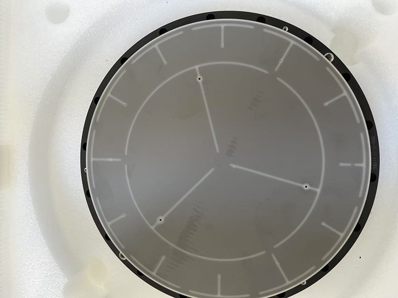
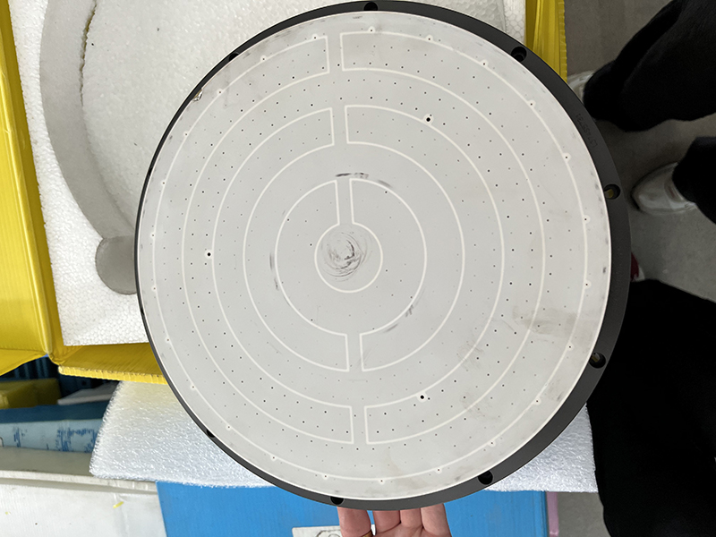
It features a sandwich-like structure: the bottom layer is a base plate for support and circuit integration, the middle layer consists of metal electrodes (unipolar, bipolar or multipolar), and the surface layer is covered with an insulating and thermally conductive dielectric layer made of materials such as aluminum nitride and aluminum oxide. During operation, the workpiece acts as the upper plate of a capacitor, the built-in electrode as the lower plate, and the dielectric layer as the insulating medium, forming a complete capacitive structure that lays the foundation for electric field generation.
In practical applications, the adsorption force is mainly derived from three mechanisms, each adapted to the needs of different scenarios. First is Coulomb force adsorption, applicable to ideal insulating dielectric layers. When a high-voltage DC voltage is applied, the electrode generates an electric field that induces opposite charges on the back of the workpiece, and the Coulomb force generated by the opposite charges achieves adsorption. This mechanism delivers uniform adsorption force, prevents workpiece deformation, and is suitable for processes requiring high flatness. The magnitude of the Coulomb force is positively correlated with the dielectric constant, applied voltage and adsorption area, and negatively correlated with the thickness of the dielectric layer. Second is Johnson-Rahbek (J-R) force adsorption, the mainstream industrial mechanism, suitable for doped semiconductor dielectric layers (with weak leakage current). Charges accumulate in tiny gaps at the contact surface to form a micro electric field, and the resultant force is the J-R force. This mechanism requires a lower voltage (500-800V) and generates a stronger adsorption force, which can overcome the pressure of helium cooling and adapt to minor roughness on the contact surface. Third is gradient force adsorption, commonly seen in designs with alternating multi-electrode arrangement. Positive and negative electrodes form a non-uniform electric field, and the unidirectional resultant force is generated by the stress difference on both sides of the workpiece. The adsorption force can be enhanced by optimizing electrode spacing and dielectric layer thickness, making it suitable for workpieces with special shapes.
Taking the semiconductor etching process as an example, the complete working process is divided into three steps, which simultaneously realize workpiece fixation and temperature control. Step 1: Workpiece Positioning – The wafer is transferred to the surface of the chuck’s dielectric layer and adjusted to the fitting position. Step 2: Electrostatic Adsorption – The controller applies a set voltage to the electrodes (plasma assistance is required for workpiece charging in unipolar mode, while the workpiece is directly polarized in bipolar mode), and adsorption is achieved via Coulomb force or J-R force. The adsorption force must be greater than the backside helium cooling pressure to ensure firm fixation. Step 3: Processing and Release – During processing, the dielectric layer conducts heat, and the wafer temperature is regulated by coordinating helium gas with the built-in cooling system. After processing, the voltage is cut off and a reverse static elimination voltage is applied to eliminate residual charges and avoid workpiece adhesion, followed by wafer transfer.
Based on the non-contact adsorption principle, the ESC Electrostatic Chuck fundamentally solves the problems of scratches and deformation caused by traditional mechanical clamping, as well as the failure of vacuum adsorption in ultra-high vacuum environments. At the same time, the material characteristics of the dielectric layer and the multi-zone electrode design enable uniform temperature control to be realized synchronously during the adsorption process, perfectly meeting the stringent requirements for precision and stability of core semiconductor processes such as plasma etching, ion implantation and thin film deposition.