What Factors Affect The Adsorption Force Of ESC Electrostatic Chucks?
Release time:2026-01-23
Visits:277
The core factors influencing the adsorption force of ESC Electrostatic Chucks can be categorized into four types: material characteristics, structural parameters, operating parameters and working environment. These factors are interrelated and directly determine the stability, uniformity and adaptability of adsorption, with a detailed analysis as follows:
1. Material Characteristics
Materials form the fundamental guarantee for adsorption force, and their core impact lies in the effect of charge conduction and electric field formation.
Dielectric layer material and performance
The dielectric constant and volume resistivity of the dielectric layer directly determine the adsorption mechanism and the magnitude of adsorption force. A higher dielectric constant results in a stronger electric field and greater adsorption force (especially Coulomb force); aluminum nitride ceramics have a higher dielectric constant than aluminum oxide and deliver better adsorption performance. The volume resistivity must be precisely matched to the adsorption mechanism: for J-R force chucks, it should be controlled within the range of 10⁹–10¹²Ω·cm. Excessively high resistivity will make the chuck tend to exhibit Coulomb force characteristics (weak adsorption force and high voltage requirement), while excessively low resistivity will cause excessive leakage current and subsequent attenuation of adsorption force. In addition, the purity and compactness of the dielectric layer affect charge accumulation capacity; impurities or pores can cause electric field distortion and reduce local adsorption force.
Dielectric layer thickness
Adsorption force is negatively correlated with the thickness of the dielectric layer (adsorption force ∝1/d² in the Coulomb force formula). A thinner layer leads to more concentrated electric field intensity and stronger adsorption force, but an overly thin layer will reduce insulation performance and increase the risk of breakdown. A balance must therefore be struck in combination with voltage parameters, with the conventional industrial thickness ranging from 0.1 to 0.5mm.
Workpiece material characteristics
The electrical conductivity and dielectric properties of the workpiece affect the efficiency of charge induction. Conductive/semiconductor workpieces can induce charges rapidly and ensure stable adsorption force; insulating workpieces have a slow charge induction speed and require matching with specific electrode designs (e.g., multipolar) to enhance adsorption. Porous or rough-surfaced workpieces reduce the effective contact area and weaken local adsorption force, which needs to be compensated for through surface microstructure optimization.
2. Structural Design Factors
Structural parameters determine the electric field distribution and force conduction efficiency, with a core focus on electrodes and overall precision.
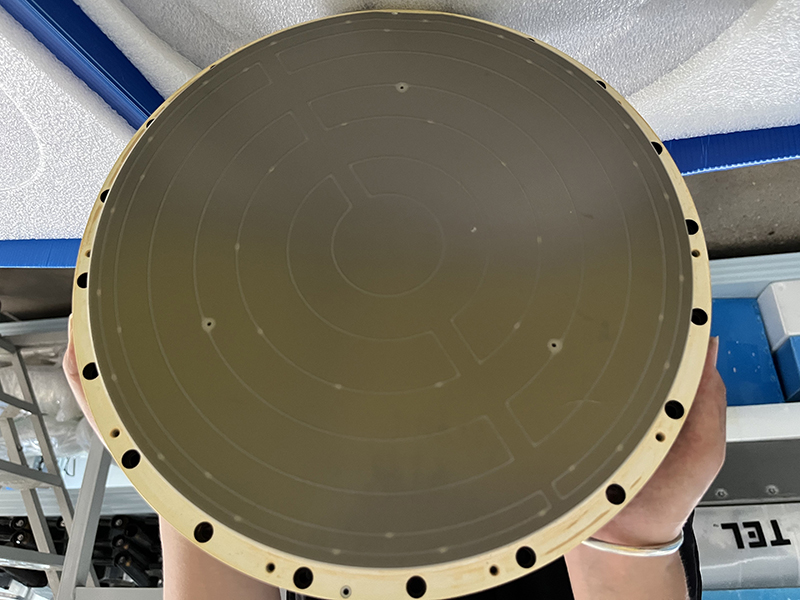
Electrode design
Electrode types (unipolar/bipolar/multipolar) affect the electric field coverage. Unipolar electrodes feature concentrated electric fields and strong adsorption force (superior to bipolar electrodes at the same voltage) but poor uniformity; bipolar/multipolar electrodes enable more uniform electric field distribution but require a reduced electrode spacing to compensate for adsorption force. The number of electrodes and arrangement density (e.g., interdigitated electrode spacing) directly impact local adsorption force—the smaller the spacing, the more obvious the electric field superposition effect and the more concentrated the adsorption force. In addition, the electrical conductivity of electrode materials (copper, tungsten, etc.) affects the electric field response speed and indirectly impacts the efficiency of adsorption force establishment.
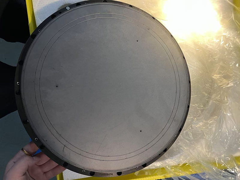
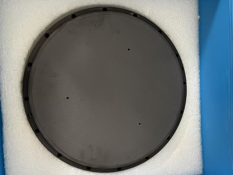
Adsorption surface precision
Deviations in the global flatness and parallelism of the adsorption surface can lead to uneven workpiece fitting, excessively large local contact gaps, electric field leakage and attenuation of adsorption force. In semiconductor processes, when flatness exceeds 1μm and parallelism exceeds 5μm, insufficient edge adsorption force and workpiece warpage are likely to occur, requiring precision control within standard ranges.
Structural sealing performance
For vacuum and helium cooling working conditions, the sealing structure of the chuck affects gas leakage. Excessively high backside helium pressure can offset part of the adsorption force. It is therefore necessary to reduce gas permeation through optimized sealing designs (e.g., sealing ring materials and groove structures) to ensure stable adsorption force.
3. Operating Parameter Factors
Operating parameters directly regulate the magnitude and stability of adsorption force, with a core focus on voltage, temperature control and static elimination settings.
Applied voltage
Adsorption force is positively correlated with the square of the applied voltage (a rule followed by both Coulomb force and J-R force)—the higher the voltage, the stronger the adsorption force. However, the voltage must match the insulation capacity of the dielectric layer to avoid breakdown. Coulomb force chucks require a high voltage of 3000–4000V, while J-R force chucks only need a low voltage of 500–800V. Overvoltage operation will accelerate the aging of the dielectric layer and instead reduce the stability of adsorption force.
Voltage application duration and mode
Long-term voltage application is prone to charge accumulation, leading to an increase in residual adsorption force, but excessive accumulation will cause local electric field saturation and a slowdown in the growth of adsorption force. The pulse voltage application mode can reduce charge accumulation and improve the controllability of adsorption force, making it more suitable for long-term working conditions than DC voltage.
Temperature control
Excessively high process temperatures reduce the resistivity of the dielectric layer, increase leakage current and weaken adsorption force; excessively low temperatures slow down charge migration speed and prolong the establishment time of adsorption force. Meanwhile, uneven temperature distribution leads to differences in dielectric layer performance and unbalanced adsorption force distribution. It is therefore necessary to maintain temperature stability through multi-zone temperature control and high thermal conductivity dielectric layers.
4. Working Environment Factors
The external environment indirectly alters adsorption force by affecting material performance and electric field stability.
Vacuum degree
An ultra-high vacuum environment (10⁻⁵ Pa and below) reduces the concentration of gas molecules adsorbed on the dielectric layer surface, decreases charge loss, and results in a slightly higher adsorption force than in the atmospheric environment. However, the breakdown voltage of the dielectric layer decreases under vacuum, requiring a reduction in operating voltage to avoid risks, which indirectly impacts the upper limit of adsorption force.
Plasma environment
Plasma in processes such as etching and ion implantation bombards the dielectric layer surface, leading to increased surface roughness and attenuation of dielectric performance, which will cause a gradual decline in adsorption force with long-term use. At the same time, plasma can assist in charging the workpiece of unipolar chucks and improve adsorption force. A balance must therefore be struck between the effects of plasma bombardment and auxiliary charging.
Environmental impurities and humidity
In the atmospheric environment, dust and particles block the contact between the workpiece and the dielectric layer, reducing the effective adsorption area; high humidity reduces the insulation of the dielectric layer, increases leakage current and weakens adsorption force. The chuck thus needs to be used in conjunction with an ultra-clean and low-humidity environment.