Wafer Transfer Robot End Effectors And Edge-Grip Considerations For Semiconductor Tool
Release time:2026-10-26
Visits:125
What Is a Wafer Transfer Robot End Effector?
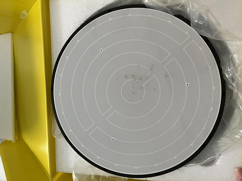
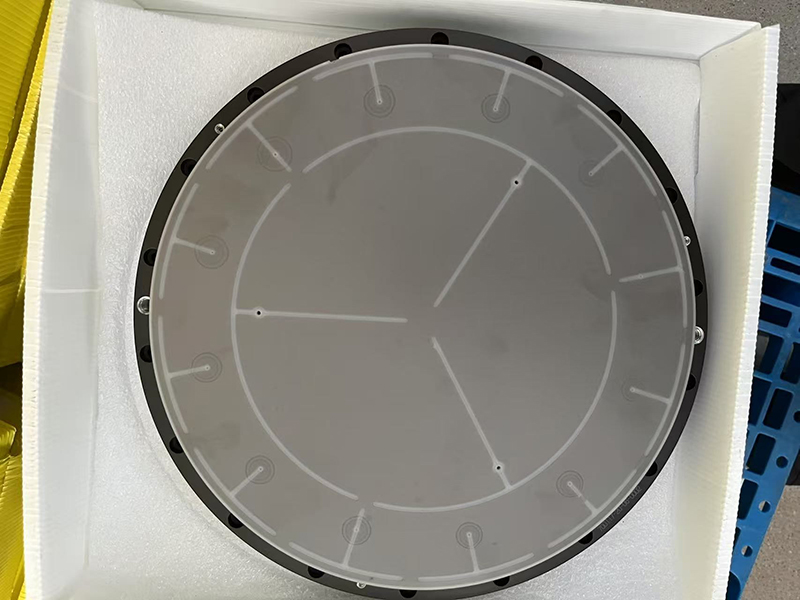
A wafer transfer robot end effector is the wafer-handling "hand" attached to the robot arm that grips (or non-contact lifts) a silicon wafer during transfer between load lock, transfer chamber, and process chambers in a semiconductor cluster tool. The end effector is typically made of ceramic (Al₂O₃, ZrO₂) or anodized aluminum with vacuum-compatible O-ring seals and is designed for ISO Class 3 cleanroom service.
Typical WTR end effector applications:
Load lock to transfer chamber pickup / place.
Transfer chamber to process chamber pickup / place.
Process chamber to buffer chamber pickup / place.
Wafer mapping / inspection station pickup / place.
Cooling station pickup / place.
Pre-aligner pickup / place.
The end effector is one of the most-stressed components in the cluster tool because it makes thousands of wafer contacts per day and must maintain zero particle generation and zero micro-scratch through the entire production cycle.
What Are the End Effector Types?
The main end effector types are mechanical edge-grip (fork-style, with two or three contact points), Bernoulli non-contact (gas-cushion lift), and vacuum edge-grip (suction at the wafer edge). Each type provides a different balance of wafer protection, throughput, and reliability.
|
End effector type |
Mechanism |
Wafer protection |
Throughput |
|
Mechanical edge-grip |
Two or three contact points at wafer edge |
Edge contact zone, no center contact |
Fast (< 1 s) |
|
Bernoulli non-contact |
Gas cushion lifts wafer |
No contact |
Slower (> 1 s) |
|
Vacuum edge-grip |
Vacuum suction at wafer edge |
Edge contact zone |
Fast (< 1 s) |
|
Pneumatic edge-grip |
Air bladder expansion under wafer edge |
Edge contact zone |
Fast (< 1 s) |
For production 300 mm tools, mechanical edge-grip is the standard because it provides fast cycle, reliable pickup, and compatibility with all wafer types (silicon, sapphire, GaAs).
How Does a Mechanical Edge-Grip Work?
A mechanical edge-grip end effector uses two or three contact points (typically at the wafer edge exclusion zone, 1–3 mm from the edge) to support the wafer from below, with the contact points designed to apply minimum force while preventing wafer slip during acceleration / deceleration of the robot arm. The contact geometry is critical to avoid micro-scratches and edge chipping.
|
Edge-grip feature |
Function |
|
Contact points (typ. 2 or 3) |
Support wafer from below |
|
Contact zone |
1–3 mm from wafer edge (edge exclusion) |
|
Contact material |
Ceramic (Al₂O₃) or anodized Al |
|
Contact area |
< 1 cm² per contact |
|
Pickup force |
5–20 N (typ) per contact |
|
Pick / place time |
< 0.5 s per wafer |
For thin wafers (< 100 μm), the contact area and force are reduced to prevent wafer bow and breakage. For warped wafers, special end effectors with compliant contact are used.
What Is the Wafer Edge Exclusion Zone?
The wafer edge exclusion zone (EEZ) is the outer annulus of the wafer (typ. 1–3 mm for 300 mm) where devices are not patterned because of mechanical and process damage during handling and processing. The end effector contact points must land in the EEZ to avoid contacting active devices.
|
Wafer size |
Edge exclusion zone |
Notes |
|
150 mm |
2 mm |
Legacy |
|
200 mm |
2 mm |
Standard |
|
300 mm |
2 mm (typ.), 3 mm (advanced node) |
Standard, advanced |
|
450 mm (proposed) |
3 mm |
Future |
For advanced-node (sub-3 nm) production, the EEZ is expanding to 3 mm to protect edge devices from handling damage.
How Does a Bernoulli Non-Contact End Effector Work?
A Bernoulli non-contact end effector uses a controlled gas (typ. N₂ or clean dry air) flow through an annular slot to create a low-pressure region above the slot, lifting the wafer on a thin gas cushion without physical contact. The non-contact mechanism eliminates micro-scratches but requires longer pickup time and precise gap control.
|
Bernoulli parameter |
Typical value |
|
Gas pressure |
0.5–2 bar |
|
Gas flow |
1–5 slm |
|
Lift gap |
50–200 μm |
|
Lift time |
1–3 s |
|
Wafer size |
200, 300 mm |
Bernoulli end effectors are used for ultra-thin wafers (< 50 μm), warped substrates, and sensitive materials where edge-grip contact is unacceptable.
What Are the Particle and Defectivity Requirements?
End effectors must add < 3 particles @ ≥ 50 nm per wafer pickup to maintain ISO Class 3 cleanroom wafer defectivity, with the dominant particle sources being the contact surfaces, the vacuum O-ring seals, and the robot arm friction. Particle control is achieved by material selection, surface finish, and actuation cleanliness.
|
Particle source |
Mitigation |
|
Contact surface |
Ra ≤ 0.4 μm, ceramic |
|
Vacuum O-ring |
FFKM (Kalrez), low-shedding |
|
Robot arm friction |
Edge seal, bellows |
|
Particulate shedding |
ISO Class 3 cleanroom assembly |
|
Particle transfer |
Material compatibility, no static |
For 300 mm advanced-node production, end effector particle addition is monitored continuously and end effectors are replaced when particle count rises above specification.
What Is the Lifetime and Failure Mode?
End effectors wear through contact-surface erosion, O-ring compression set, vacuum line degradation, and robot arm bearing wear, with typical production lifetimes of 1–3 years (10,000,000+ wafer pickups). Failure modes include wafer slip (insufficient grip), micro-scratch (surface degradation), and particle rise (O-ring shedding).
|
Failure mode |
Symptom |
Cause |
|
Wafer slip |
Wafer drops during transfer |
Grip force loss, surface wear |
|
Micro-scratch |
Wafer defectivity |
Surface contamination, wear |
|
Particle rise |
Wafer defectivity |
O-ring shedding, surface erosion |
|
Vacuum leak |
Wafer slip, slow pickup |
O-ring aging |
|
Position drift |
Misalignment, wafer crash |
Bearing wear, calibration loss |
Hitron's Product page lists wafer-handling components and the Application page describes process integration.
How Is the End Effector Cleaned?
End effectors are cleaned in-situ (between-wafer N₂ purge or plasma clean) and ex-situ (periodic wet clean or UV-ozone) to remove particle and organic contamination, with the cleaning protocol matched to the wafer defectivity requirement. In-situ N₂ purge is standard for production tools.
|
Cleaning type |
Frequency |
Method |
|
In-situ N₂ purge |
Every wafer |
N₂ blow-off at pickup / place |
|
In-situ plasma |
Daily |
O₂ plasma clean |
|
Ex-situ wet clean |
Weekly to monthly |
Manual with IPA, DI water |
|
Ex-situ UV-ozone |
Monthly |
Surface organic removal |
For ISO Class 3 production tools, end effector cleaning is monitored continuously and is replaced when cleaning can no longer maintain particle specification.
How Does the End Effector Interface to the Robot?
The end effector mounts to the robot arm via a standard mechanical interface (typically a vacuum flange with KF / CF / ISO-K clamp) with the vacuum line providing the grip force and the electrical line providing the position sensor feedback. The interface must be vacuum-compatible and allow end effector replacement without breaking chamber vacuum.
|
Interface |
Function |
|
Mechanical flange |
End effector mounting |
|
Vacuum line |
Grip force |
|
Position sensor |
Wafer presence detection |
|
Cleaning gas |
N₂ purge line |
|
Heater (optional) |
Wafer pre-heating |
For service, the end effector is typically replaced as a unit to minimize downtime. Hitron's Product page lists compatible end effectors and replacement parts.
What Is the Standard Wafer Mapping?
Wafer mapping is the process of measuring wafer position, notch / flat orientation, and centering before pickup / place, with the mapping performed by optical sensors or through-beam detectors on the end effector or pre-aligner station. Wafer mapping prevents mis-orientation and mis-pickup.
|
Mapping method |
Mechanism |
Accuracy |
|
Optical (camera) |
Vision system |
< 0.5 mm |
|
Through-beam (LED + detector) |
Shadow detection |
< 1 mm |
|
Notch / flat detector |
Optical or mechanical |
Per wafer type |
|
Pre-aligner station |
Independent station |
< 0.1 mm |
For production tools, wafer mapping is performed automatically and verified by the tool controller before each pickup / place. Mismapped wafers are rejected to the reject cassette.
Frequently Asked Questions
Q: What is a wafer transfer robot end effector?
A: A wafer transfer robot end effector is the wafer-handling "hand" attached to the robot arm that grips (or non-contact lifts) a silicon wafer during transfer between load lock, transfer chamber, and process chambers in a semiconductor cluster tool.
Q: What is the difference between mechanical edge-grip and Bernoulli non-contact?
A: Mechanical edge-grip uses two or three contact points at the wafer edge to support the wafer. Bernoulli non-contact uses a gas cushion to lift the wafer without contact. Mechanical is faster and more common; Bernoulli is preferred for ultra-thin or warped wafers.
Q: What is the typical end effector lifetime?
A: 1–3 years (10,000,000+ wafer pickups) in production 300 mm tools. Replaced at preventive maintenance based on wafer defectivity rise.
Q: Can end effectors be repaired?
A: Contact surfaces can be refurbished (re-grinding, re-coating) but most production end effectors are replaced as units to minimize downtime.
Q: What material is used for the contact surface?
A: Ceramic (Al₂O₃ or ZrO₂) or hard-anodized aluminum. Ceramic is preferred for ISO Class 3 cleanroom service because of low particle generation.
Q: How is the end effector cleaned?
A: In-situ N₂ purge (every wafer), in-situ plasma clean (daily), ex-situ wet clean (weekly to monthly), and ex-situ UV-ozone (monthly). Cleaning protocol matched to wafer defectivity requirement.
Q: Does Hitron supply wafer transfer robots?
A: Hitron's Product page lists front-end equipment components including wafer-handling components. Contact the Hitron engineering team for specific wafer transfer robot and end effector requirements.
Q: What is the wafer edge exclusion zone?
A: The outer annulus of the wafer (typ. 1–3 mm for 300 mm) where devices are not patterned because of mechanical and process damage. End effector contact must land in this zone.
Q: What is the maximum wafer size for standard end effectors?
A: Standard end effectors support 200 mm and 300 mm wafers. For 450 mm (proposed future generation), special end effectors are required.
Conclusion
The wafer transfer robot end effector is the wafer-handling component that enables all wafer movement in a semiconductor cluster tool, with mechanical edge-grip being the standard for production 300 mm tools and Bernoulli non-contact reserved for ultra-thin or warped wafers. End effector design affects wafer defectivity, throughput, and reliability, with ceramic contact surfaces and FFKM seals being the standard for ISO Class 3 cleanroom service. Hitron's Product page lists the front-end equipment component range including wafer-handling components, with the Electrostatic Chuck family providing wafer clamping and the Slit Valve Door family providing chamber isolation during transfer. For product range, certifications, and engineering support, consult the About Us and Contact Us pages.