What Is An Electrostatic Chuck? An Analysis Of The Invisible Hand In Semiconductor Precision Manufacturing
Release time:2026-07-13
Visits:319
In precision manufacturing fields such as semiconductors and display panels, achieving damage-free, high-precision clamping of workpieces is one of the key issues determining process yield. The Electrostatic Chuck (ESC or E-Chuck), a device based on the principle of electrostatic adsorption, has become the invisible support of the industry with its unique advantages, known as the invisible hand of semiconductor processes.
Core Functions of Electrostatic Chucks: Solving Clamping Pain Points in Precision Manufacturing
The value of electrostatic chucks lies in solving many bottlenecks of traditional clamping technologies with invisible force, and their core functions revolve around high precision, low pollution, and strong adaptability:
1. Ultra-clean Clamping: Eliminating Contamination at the Source
Traditional mechanical clamping can cause physical contact scratches, while vacuum adsorption may leave particles—these issues can directly lead to chip scrapping for semiconductor wafers that require zero contamination. Electrostatic chucks achieve non-contact adsorption through electrostatic force, without physical contact with the workpiece surface throughout the process, completely avoiding contact contamination and particle residue, perfectly adapting to the ultra-clean standards of semiconductor manufacturing.
2. Uniform Adsorption Force: Ensuring Workpiece No Deformation
Precision workpieces such as wafers and optical components have extremely high requirements for flatness; even slight warping can affect subsequent process accuracy. The uniform distribution of adsorption force of electrostatic chucks allows the workpiece to maintain a stable flat state, effectively preventing warping or deformation, providing a foundation for the high-precision implementation of processes such as etching and deposition.
3. Adaptability to Extreme Environments: Stabilizer in Vacuum
In semiconductor processes such as Extreme Ultraviolet Lithography (EUVL) and plasma processing, equipment is often in a high-vacuum environment—traditional vacuum chucks fail as they cannot form a pressure difference, while electrostatic chucks rely on the action of electrostatic fields, maintaining stable adsorption even in vacuum or plasma environments, becoming an essential tool for these high-end processes.
4. Precise Temperature Control: Adapting to Complex Process Requirements
Many semiconductor processes require temperature control precise to ±1℃. Electrostatic chucks can accurately adjust the surface temperature of workpieces (such as wafers) through a built-in backside gas system, meeting the temperature control needs of different processes and further ensuring process consistency.
Main Application Scenarios of Electrostatic Chucks: Covering Core Links of Precision Manufacturing
From semiconductor chips to optical components, the application of electrostatic chucks has penetrated into key scenarios of precision manufacturing:
1. Semiconductor Manufacturing: Fixator for Key Processes
In core semiconductor processes such as etching (ETCH), Chemical Vapor Deposition (CVD), Physical Vapor Deposition (PVD), and Ion Implantation (IMP), electrostatic chucks fix wafers, ensuring they remain stable during high-speed rotation, plasma impact, etc., directly affecting chip yield and performance.
2. Panel Display and Optical Processing: Preferred for Damage-free Clamping
Workpieces such as liquid crystal panels and optical lenses have extremely high requirements for surface integrity. The non-contact adsorption of electrostatic chucks avoids edge indentation or surface scratches, reduces the edge effect (i.e., process differences between the workpiece edge and center), and improves product consistency.
3. High-vacuum Processes: Dependence of High-end Processes like EUVL
Extreme Ultraviolet Lithography (EUVL), as the core technology for semiconductor processes of 7nm and below, must be carried out in a high-vacuum environment—only electrostatic chucks can stably adsorb wafers at this time, ensuring lithography precision and becoming a core component of EUVL equipment.
Technical Classification of Electrostatic Chucks: Adaptive Choices for Different Scenarios
According to different principles and materials, electrostatic chucks are mainly divided into two categories:
1. Classification by Adsorption Principle: Coulomb vs J-R Type
- Coulomb type: Relies on pure electrostatic adsorption, suitable for high-impedance ceramic dielectric layers, with uniform but relatively small adsorption force, commonly used in scenarios with moderate adsorption force requirements;
- J-R type: Combines electrostatic and micro-current effects, with stronger adsorption force and better thermal conductivity, suitable for high-end processes requiring strong adsorption + high thermal conductivity (such as high-temperature deposition).
2. Classification by Material: Aluminum Oxide vs Aluminum Nitride
Mainstream electrostatic chucks use ceramics as dielectric layer materials:
- Aluminum oxide ceramics: Lower cost, suitable for mid-to-low-end processes;
- Aluminum nitride ceramics: Thermal conductivity is 5-10 times that of aluminum oxide, enabling rapid heat transfer from the workpiece, becoming the preferred material for high-end semiconductor processes (such as EUVL).
Electrostatic Chuck vs Traditional Technologies: Why It is the Better Solution?
Compared with traditional technologies such as mechanical clamping and vacuum adsorption, the advantages of electrostatic chucks lie in long-term value:
- Pollution control: Non-contact adsorption reduces particle contamination, and wafer yield can be increased by 5%-10% (according to industry data);
- Process compatibility: Adapts to extreme environments such as high temperature, vacuum, and plasma, supporting more complex process upgrades;
- Long-term cost: Although the initial purchase cost is higher than traditional chucks, electrostatic chucks have a long service life (up to several years) and simple maintenance, resulting in lower overall cost.
Conclusion: The Invisible Promoter of Precision Manufacturing
From the miniaturization of semiconductor chips to the high definition of display panels,
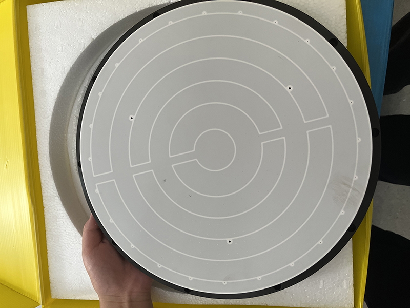
electrostatic chucks, as the invisible hand, silently support every step of progress in precision manufacturing. Its technological breakthroughs (such as the application of aluminum nitride materials and the improvement of adsorption force uniformity) have directly promoted semiconductor processes from 14nm to 7nm, 5nm, and even 3nm.
For the precision manufacturing industry, electrostatic chucks are not only a tool but also a core support for achieving higher precision and better yield—and this is why it is called the invisible hand of semiconductor processes.